- 您现在的位置:买卖IC网 > Sheet目录443 > IRF510STRLPBF (Vishay Siliconix)MOSFET N-CH 100V 5.6A D2PAK
�� �
�
�IRF510S,� SiHF510S�
�Vishay� Siliconix�
�Power� MOSFET�
�PRODUCT� SUMMARY�
�FEATURES�
�?� Halogen-free� According� to� IEC� 61249-2-21�
�V� DS� (V)�
�R� DS(on)� (� ?� )�
�Q� g� (Max.)� (nC)�
�Q� gs� (nC)�
�Q� gd� (nC)�
�Configuration�
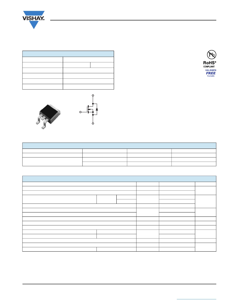
�D� 2� PAK� (TO-263)�
�V� GS� =� 10� V�
�100�
�8.3�
�2.3�
�3.8�
�Single�
�D�
�0.54�
�Definition�
�?� Surface� Mount�
�?� Available� in� Tape� and� Reel�
�?� Dynamic� dV/dt� Rating�
�?� Repetitive� Avalanche� Rated�
�?� 175� °C� Operating� Temperature�
�?� Fast� Switching�
�?� Ease� of� Paralleling�
�?� Compliant� to� RoHS� Directive� 2002/95/EC�
�DESCRIPTION�
�Third� generation� Power� MOSFETs� from� Vishay� provide� the�
�designer� with� the� best� combination� of� fast� switching,�
�ruggedized� device� design,�
�low� on-resistance� and�
�G�
�cost-effectiveness.�
�The� D� 2� PAK� (TO-263)� is� a� surface� mount� power� package�
�capable� of� accommodating� die� sizes� up� to� HEX-4.� It�
�provides� the� highest� power� capability� and� the� lowest�
�G� D�
�S�
�S�
�N-Channel� MOSFET�
�possible� on-resistance� in� any� existing� surface� mount�
�package.� The� D� 2� PAK� (TO-263)� is� suitable� for� high� current�
�applications� because� of� its� low� internal� connection�
�resistance� and� can� dissipate� up� to� 2.0� W� in� a� typical� surface�
�mount� application.�
�ORDERING� INFORMATION�
�Package�
�Lead� (Pb)-free� and� Halogen-free�
�Lead� (Pb)-free�
�D� 2� PAK� (TO-263)�
�SiHF510S-GE3�
�IRF510SPbF�
�SiHF510S-E3�
�D� 2� PAK� (TO-263)�
�SiHF510STRL-GE3� a�
�IRF510STRLPbF� a�
�SiHF510STL-E3� a�
�D� 2� PAK� (TO-263)�
�SiHF510STRR-GE3� a�
�IRF510STRRPbF� a�
�SiHF510STR-E3� a�
�Note�
�a.� See� device� orientation.�
�ABSOLUTE� MAXIMUM� RATINGS� (T� C� =� 25� °C,� unless� otherwise� noted)�
�PARAMETER�
�Drain-Source� Voltage�
�Gate-Source� Voltage�
�SYMBOL�
�V� DS�
�V� GS�
�LIMIT�
�100�
�±� 20�
�UNIT�
�V�
�Continuous� Drain� Current�
�V� GS� at� 10� V�
�T� C� =� 25� °C�
�T� C� =� 100� °C�
�I� D�
�5.6�
�4.0�
�A�
�Pulsed� Drain� Current� a�
�I� DM�
�20�
�Linear� Derating� Factor�
�Linear� Derating� Factor� (PCB� Mount)� e�
�0.29�
�0.025�
�W/°C�
�Single� Pulse� Avalanche� Energy� b�
�Avalanche� Current� a�
�Repetitive� Avalanche� Energy� a�
�E� AS�
�I� AR�
�E� AR�
�100�
�5.6�
�4.3�
�mJ�
�A�
�mJ�
�Maximum� Power� Dissipation�
�Maximum� Power� Dissipation� (PCB� Mount)� e�
�Peak� Diode� Recovery� dV/dt� c�
�Operating� Junction� and� Storage� Temperature� Range�
�Soldering� Recommendations� (Peak� Temperature)�
�T� C� =� 25� °C�
�T� A� =� 25� °C�
�for� 10� s�
�P� D�
�dV/dt�
�T� J� ,� T� stg�
�43�
�3.7�
�5.5�
�-� 55� to� +� 175�
�300� d�
�W�
�V/ns�
�°C�
�Notes�
�a.� Repetitive� rating;� pulse� width� limited� by� maximum� junction� temperature� (see� fig.� 11).�
�b.� V� DD� =� 25� V,� starting� T� J� =� 25� °C,� L� =� 4.8� mH,� R� g� =� 25� ?� ,� I� AS� =� 5.6� A� (see� fig.� 12).�
�c.� I� SD� ?� 5.6� A,� dI/dt� ?� 75� A/μs,� V� DD� ?� V� DS� ,� T� J� ?� 175� °C.�
�d.� 1.6� mm� from� case.�
�e.� When� mounted� on� 1"� square� PCB� (FR-4� or� G-10� material).�
�*� Pb� containing� terminations� are� not� RoHS� compliant,� exemptions� may� apply�
�Document� Number:� 91016�
�S11-1044-Rev.� C,� 30-May-11�
�www.vishay.com�
�1�
�This� document� is� subject� to� change� without� notice.�
�THE� PRODUCTS� DESCRIBED� HEREIN� AND� THIS� DOCUMENT� ARE� SUBJECT� TO� SPECIFIC� DISCLAIMERS,� SET� FORTH� AT� www.vishay.com/doc?91000�
�发布紧急采购,3分钟左右您将得到回复。
相关PDF资料
IRF510
MOSFET N-CH 100V 5.6A TO-220AB
IRF520NSTRR
MOSFET N-CH 100V 9.7A D2PAK
IRF520N
MOSFET N-CH 100V 9.7A TO-220AB
IRF520SPBF
MOSFET N-CH 100V 9.2A D2PAK
IRF5210L
MOSFET P-CH 100V 40A TO-262
IRF5305L
MOSFET P-CH 55V 31A TO-262
IRF530A
MOSFET N-CH 100V 14A TO-220
IRF530NL
MOSFET N-CH 100V 17A TO-262
相关代理商/技术参数
IRF510STRR
功能描述:MOSFET N-Chan 100V 5.6 Amp RoHS:否 制造商:STMicroelectronics 晶体管极性:N-Channel 汲极/源极击穿电压:650 V 闸/源击穿电压:25 V 漏极连续电流:130 A 电阻汲极/源极 RDS(导通):0.014 Ohms 配置:Single 最大工作温度: 安装风格:Through Hole 封装 / 箱体:Max247 封装:Tube
IRF510STRRPBF
功能描述:MOSFET N-Chan 100V 5.6 Amp RoHS:否 制造商:STMicroelectronics 晶体管极性:N-Channel 汲极/源极击穿电压:650 V 闸/源击穿电压:25 V 漏极连续电流:130 A 电阻汲极/源极 RDS(导通):0.014 Ohms 配置:Single 最大工作温度: 安装风格:Through Hole 封装 / 箱体:Max247 封装:Tube
IRF511
制造商:Rochester Electronics LLC 功能描述: 制造商:Freescale Semiconductor 功能描述:SUB ONLY ON SEMICONDUCTOR
IRF511R
制造商:未知厂家 制造商全称:未知厂家 功能描述:TRANSISTOR | MOSFET | N-CHANNEL | 80V V(BR)DSS | 5.6A I(D) | TO-220AB
IRF512
制造商:Rochester Electronics LLC 功能描述:- Bulk
IRF512R
制造商:未知厂家 制造商全称:未知厂家 功能描述:TRANSISTOR | MOSFET | N-CHANNEL | 100V V(BR)DSS | 4.9A I(D) | TO-220AB
IRF512S2532
制造商:Rochester Electronics LLC 功能描述:- Bulk
IRF513
制造商:Distributed By MCM 功能描述:SUB ONLY MOSFET TO-220AB N-CH80V 4.9A 43W GDS *SS